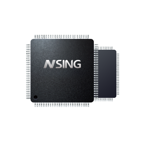
• CPU Core
― 32-bit ARM Cortex-M4F + FPU, single-cycle hardware multiplication and division instruction, support DSP instruction and MPU
― Built-in 8-KB instruction Cache supporting Flash acceleration unit for zero-wait program execution
―Frequency up to 240 MHz, 300 DMIPS
• Memories
― 512-KByte of embedded Flash memory with ECC
♦ Supports encryption, multi-user partition and data protection
♦ 10,000 erase/write cycles and 10-years data retention
― 160-KByte of general SRAM with hardware parity checking
― 32-KByte of CCM SRAM with ECC, defaults to general SRAM after power-up, configurable as CCM SRAM
― 4-KByte of Backup SRAM with ECC available in Standby mode
• Power Modes
― Run mode: 45 mA/MHz@240 MHz (peripherals off, 3.3 V@25℃)
― Stop0 mode: SRAM and all registers can be configured to retention, RTC run
― Standby mode: 6uA, all backup registers and Backup SRAM retained, all IOs retained, optional RTC run
― VBAT mode: 4uA, all backup registers and Backup SRAM retained, optional RTC run
• Clock
― HSE: 4MHz~32MHz high-speed external crystal oscillator
― LSE: 32.768KHz low-speed external crystal oscillator
― Built-in multiple high speed PLLs
― MCO: Supports 2-channel clock outputs, which can be configured independently as clock output
― HSI: High-speed internal RC 8MHz, -1.5% to +2% accuracy (full temperature range)
― LSI: Low-speed internal RC 32KHz, +/-10% accuracy (full temperature range)
• Reset
― Supports power-on/brown-out/external pin reset
― Supports watchdog reset
― Supports programmable voltage detection
• GPIOs
― Up to 118 GPIOs
• Communication Interfaces
― 1x USB2.0 FS Device interface, built-in PHY, supports crystal-less mode
― 6x SPI interfaces, 2x I2S interfaces, support half/full duplex mode, multiplexed with SPI interfaces
― U(S)ART interfaces
♦ 4x USART interfaces (support ISO7816, IrDA, LIN)
♦ 4x UART interfaces
♦ TX/RX of USART3/UART5/UART8 can be mapped to all pins
― 4x I2C interfaces(Master/Slave) with speed up to 1 MHz where slave mode support dual address response
― 3x CAN-FD bus interface, TX/RX can be mapped to all pins
― 1x IEEE-802.3-2002 compatible Ethernet MAC interface, supports 10M/100M Ethernet, IEEE1588
synchronized Ethernet protocol
― 1x DVP (Digital Video Port) supporting 8/10/12/16 bit data
• High Performance Analog Interfaces
― 4x 12bit ADCs with 4.7Msps
♦ Multiple precision configuration, support 12-bit, 10-bit, 8-bit, 6-bit sampling precision, resolution up to 16-bit with hardware oversample
♦ Up to 16 external single-ended input channels, 3 internal single-ended input channels, support differential mode and single-ended mode
― 8x 12bit DAC
♦ DAC1~4: Support 1 internal output channel and 1 external output channel, with a sampling rate of 1Msps. Support output channel buffered/unbuffered modes.
♦ DAC5~8: Support 1 internal output channel and 1 external output channel, with a sampling rate of 15Msps. Only support output channel buffered/unbuffered modes.
― 4x rail-to-rail PGAs, support differential mode and single-ended mode
― 7x high-speed comparators (COMP)
― Supports 1 reference voltage VREFBUF (2.048V/2.5V/2.9V configurable) ― 1x temperature sensor
• High Speed External Memory Interfaces
― 1x xSPI interface, supporting external SRAM, PSRAM and Flash, supporting XIP
― 1x FEMC (Flexible External Memory Controller) interface, supporting external SRAM, PSRAM, NOR Flash and NAND Flash, 8/16-bit data bus width configurable
― 1x SDIO interface, support SD/SDIO/MMC format
• Mathematical hardware accelerator CORDIC for motor control functions
• Built-in filter mathematical accelerator FMAC, supporting FIR, IIR filtering
• DMA Controllers
― 2x DMA controller
― Each controller supports 8 channels
― Channel source address and destination address can be configured arbitrarily
• RTC real-time clock
― Supports leap-year calendar, alarm event, periodic wake up
― Supports internal and external clock calibration
• Timers
― 1x 16bit super high-resolution timer (SHRTIM1)
♦ Supports 6x 16-bit timer units, each timer unit has 2 independent channels, with a maximum control precision of 125ps.
♦ Supports 12 independent PWM outputs or 6 pairs of complementary PWM outputs.
― 3x 16-bit advanced control timers with maximum control precision of 4.16 ns
♦ Support input capture, complementary output, quadrature encoder input etc.
♦ Each timer has 6 independent channels, 4 of which support 4 pairs of complementary PWM output.
― 10x 16-bit general purpose timers (GTIM1~10)
♦ GTIM1~7, with a maximum control precision of 5.56ns, each timer has up to 4 independent channels, each channel supports input capture, output comparison, PWM generation, and single-pulse mode output.
♦ GTIM8~10, with a maximum control precision of 4.16ns, each timer has up to 4 independent channels, each channel supports input capture, output comparison, PWM generation, and single-pulse mode output, only channel 1 supports complementary output with dead time, supports break input.
― 2x 32-bit basic timers
― 2x 16-bit low-power timer, can operate in Stop0 and Standby mode.
― 1x 24-bit SysTick timer.
― 1x 14-bit Window Watchdog (WWDG)
― 1x 12-bit Independent Watchdog (IWDG)
• Programming Methods
― Support SWD/JTAG debugging interface.
― Support UART and USB Bootloader
• Security Features
― Flash encryption, multi-user partition management unit (SMPU)
― Supports write protection (WRP), multiple read protection (RDP) levels (L0/L1/L2)
― Built-in hardware acceleration engine for cryptographic algorithm
― Supports AES/TDES, SHA, SM3, SM4, and MD5 algorithms
― True random number generator(TRNG)
― CRC16/32 operation ― Supports secure boot, program encryption download, secure firmware update
― Supports external clock failure detection, anti-tamper detection.
• 96-bit UID and 128-bit UCID
• Operating Conditions
― Operating voltage range: 1.8V~3.6V
― Operating temperature range: -40℃ ~ 105℃
― ESD: ±4KV (HBM model), ±1KV (CDM model)
― EFT: VDD (+/-4KV,level A),I/O (+/-2KV,level A)
 Medical Electronics
 Home Appliances
 Digital Power
 All
All
 Products
 Application
 Information
  Design Resources


 Global Sales Network
